Hans Wagemans, ON4CDU, on4cdu(at)uba.be and Christophe Huygens, ON4IY, on4iy(at)uba.be (This article was published in DUBUS 1/2021)
Note: click on the images on this page to enlarge them
0. Introduction
As radio amateurs, one of our objectives is to achieve successful narrow-band communications on increasingly higher frequencies. To get there, we need a signal source that is stable in frequency. We can look at this stability from both a long and a short-term perspective: the long-term perspective (> 1 second) is usually described in the time domain using the Allan deviation, and the short-term stability (< 1 second) by describing the power distribution of the source in the frequency domain – a.k.a. the phase noise. We can think of phase noise as the source jumping around the true carrier frequency – in a very fast way.
The advent of GPS-derived standards or stable surplus references such as Rubidium standards allow us to solve the long-term stability problem. It is fairly easy nowadays to be “on frequency” since we can compare our signal source with one of these (multiplied) standards, multiply the standard as in direct frequency synthesis or use the standard to lock our source to the standard, so that the (frequency or phase) difference between the two becomes minimal.
The definition as well as impact assessment of “bad” phase noise is not easy. But intuitively it is clear that, when our signal is not stable in the short term, there will be an impact on coherence and signals become harder to decode. Also, more noise will fold into the passband and equally reduce the minimum discernable signal. On the transmit side, we would like to avoid raising the background noise level for our fellow hams, as is evident from the performance of many “modern” VHF-UHF-SHF rigs followed by big amplifiers. With big PAs now also available on 10 and 24 GHz, coupled with for example the conditions of rain scatter and associated big signal levels, this is also becoming an issue on microwaves. It is important not only to get on the air, but to do so with a signal that is as clean as possible without excessive phase noise or spurs.
1. Design
Broadband agile microwave sources are very attractive. They can be readily used for a lot of our experiments. They can provide local oscillators or beacon sources and can directly implement digital modulation schemes. Also, the same building block can now be used to provide a base signal on many ham bands by using software reconfiguration, a signal that spans from a few to x0 GHz (or even to hundreds of GHz if followed by correct multiplier chains). Traditionally, these blocks were quite complex and expensive. Usually these consist of a fixed-frequency crystal oscillator around 100 MHz (DF9LN, G8ACE, …) followed by a multi-stage multiplier that needs careful tuning for the target frequency (for example DB6NT 12 GHz LO MK 4).
Advances in synthesiser technology radically change this. Chips such as the ADF5355 consist of a combination of a voltage-controlled oscillator (VCO) in the microwave range (up to 13.6 GHz using the internal doubler) and a phase locked loop (PLL) that essentially compares the oscillator output with an external reference, hereby keeping the VCO “on target”. These approaches no longer require tuned multiplier chains since the target frequency is generated directly on chip, automatically selecting one of the four integrated oscillators in the range of 3.4-6.8 GHz followed by integrated multiplication or division so that 54 to 13600 MHz is directly available at the output pin.
In practice, the phase noise resulting from the synthesiser-reference combination has three areas depending on the loop bandwidth and chip characteristics: close to the carrier the reference noise will usually dominate, quickly overtaken by “chip” noise. Outside the loop the noise of the integrated VCO is the dominating factor.
Given the existence of cheap frequency standards and the fact that the reference is only critical for a small part of the noise spectrum it is tempting to use the reference “as-is” and use it as the PLL reference frequency directly. There are however several disadvantages to this approach. First and foremost, the short term (phase noise) characteristics of the typical ham reference are not very good. Very often, the 10 MHz crystal oscillator that is being stabilized in these references is consumer-grade in the first place (for example BG7TBL GPSDO -120 dBc/Hz at 100 Hz) or just noisy (for example, Rubidium FE-5680A that often appear on Ebay was measured around -110 dBc/Hz at 100 Hz). Next, in a real-world system of a ham, these numbers will be seriously challenged by the power supply and/or reference distribution subsystems. Note that, as will be illustrated further down in this article, phase noise increases by 20log(N) in case of multiplication by N. So, when moving to 47 GHz based on a 10 MHz reference, we increase phase noise by 73 dB Whilst the PLL will keep this noise multiplication problem under control outside the loop, it may well have a practical impact close to the carrier if we don’t start out with the best reference in the first place.
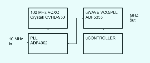
Figure1: Schematic overview of agile source
From previous, we can conclude that it would be good practice to start from the best reference available for the ADF5355. But, since we don’t necessarily have the budget for a Wenzel ULN reference oscillator, we propose here a design using general purpose low noise voltage-controlled crystal oscillator (VCXO). The VCXO is locked to a 10 MHz standard in a very narrow loop, so that the characteristics of the VCXO are not compromised. This results in the system design of figure 1.
2. Simulations
Whilst the theory of PLLs is quite complicated, we can in practice rely on a few rules of thumb and mature simulation tools. For the latter, Analog Devices (ADI) provides the free ADIsimPLL program that supports the entire range of ADI synthesisers – the chip (PLL and VCO) characteristics are already in the program which is a great help. For the basic rules, we pay attention to the following:
- Use low multiplication (N-values) because of multiplication (see above)
- Use reference divider (R values) greater than 1
- Maximise the phase detector gain and frequency
- Design the loop filter with a cut-off frequency close to the point where the VCO noise reaches the “chip” noise (typically loop bandwidth equals 1.2 times intersection).
- Use a phase margin of 45 degrees or more to achieve stability of the negative feedback
- Use a high-quality reference source with the close-in phase noise as low as possible or at least lower than the chip noise.
100 MHz reference. An ultra-low noise VCXO Crystek CVHD-950 100 MHz with very good close-in noise performance is used: -86 dBc/Hz at 10 Hz and -118 dBc/Hz at 100 Hz away from the carrier. This 100 MHz Crystek oscillator is locked with an ADF4002 PLL to a 10 MHz (GPS locked) source in a narrow loop of 10 Hz. To avoid very large capacitors in the loop filter of the ADF4002, a phase detector frequency of 1 MHz and a charge pump current of 1.25 ma have been chosen. The resulting system still has a phase noise of only -117 dBc/Hz at 100 Hz. Whilst the PLL cleans up noisy 10 MHz references, best results will be achieved with a good reference such as a Trimble Thunderbolt or a Hewlett Packard Z3801A (both with a good power supply!).
Microwave synthesiser ADF5355. A phase detector frequency (PDF) of 50 MHz was chosen. The reference source of 100 MHz is connected to the ADF5355, but a stable lock was not always obtained with a PDF of 100 MHz (note the R>1 best practice). The R divider by two in the chip gives a better shaped signal to the phase detector. The phase detector gain was maximised by setting the charge pump (CP) current to 4.8 mA. Tweaking the loop filter is a bit of an art. With a loop bandwidth of 20 kHz with a phase margin of 50 degrees was obtained. If other parameters are used, optimising with the help of ADIsimPLL is quite easy.
With these parameters an ADIsimPLL simulation run gives the results depicted in the figure.
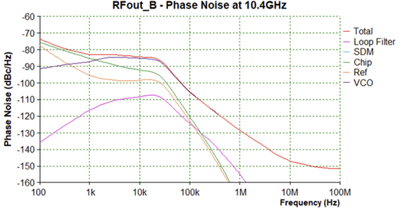
Figure 2: Simulation output of ADIsimPLL
The output of the simulation with ADIsimPLL using mentioned parameters demonstrates two points. First of all, the noise contribution of the reference is just below the chip noise. This causes the total phase noise at 100 Hz to be mainly due to chip contribution. The importance of a very low noise reference, in our case the locked Crystek (-117 dBc/Hz at 100 MHz gives -77 dBc/Hz at 10 GHz), is demonstrated. Next, inside the loop the VCO noise stays under the total noise curve (because of loop suppression) and outside the loop it determines the total noise. At the crossover point no bump is visible – so the loop filter design is satisfactory.
An obvious question upon achieving a “good” simulation is how the system performs when compared to existing solutions. The following table shows the gold standard in the field – an OCXO / multiplier combination -, an alternative agile approach we proposed 10 years ago based on both Direct Digital Synthesis (AD9912) and a multiplier, and finally the microwave wideband synthesiser.
While the microwave wideband synthesiser still underperforms around 10 kHz, it has superior performance both very close to (due to the used Crystek) and far away from (due to the absence of multiplication) the carrier. Overall, its performance is acceptable given the vastly reduced system complexity and cost, since we eliminate the multiplier chain.
| 10386 MHz phase noise (dBc/Hz) |
G8ACE+multiplier |
AD9912+multiplier |
ADF5355 |
| 100 Hz | -68 | -65 | -75 |
| 1 kHz | -90 | -85 | -82 |
| 10 kHz | -105 | -105 | -85 |
| 100 kHz | -115 | -115 | -105 |
| 1 MHz | -120 | -120 | -128 |
| 10 MHz | -138 | -138 | -148 |
3. Building
a. Take 1 – the “black” boards
The ADF5355 is only available in a 32 lead LFCSP package (the AD9912 used before has a 64 lead LFCSP). While it is certainly possible to mount the device using amateur means (paste and oven combined with some cleaning), it is quite a hassle. Therefore, we opted for the Chinese black “finished” circuit boards available amongst others on Amazon and Ebay and sold under various names and brands. They come assembled and include some low-quality SMAs.
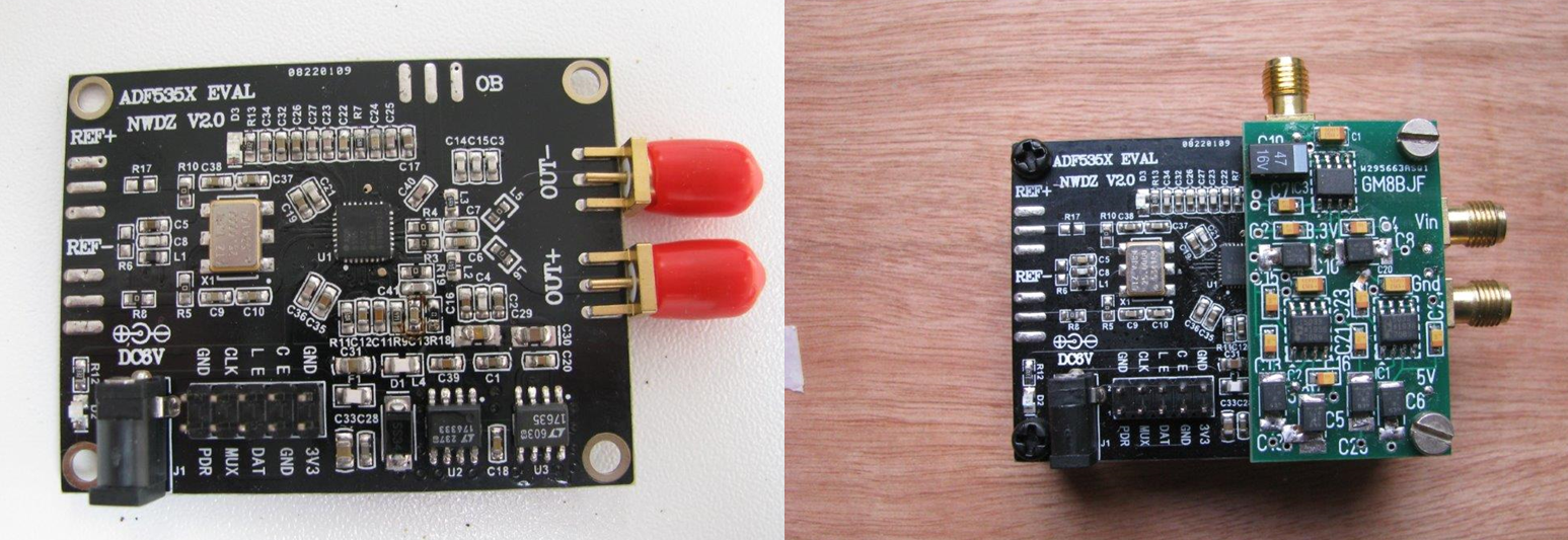
Figure 3: Used ADF “black” without and with power supply board
The schematic is a straightforward application of the datasheet, without the expensive and needed low noise power regulators and using a cheap free-running reference oscillator. As such, a first improvement is to exchange the power supply regulators on the board with high quality devices since the ones mounted are terribly noisy. The original regulators were changed to the ADM7150ARDZ family using a small circuit board designed by GM8BJF. This change resulted in a direct and dramatic improvement that can be observed even on a spectrum analyser. Clearly, unmodified boards should not be on the air – although they can be useful in a lab setting.
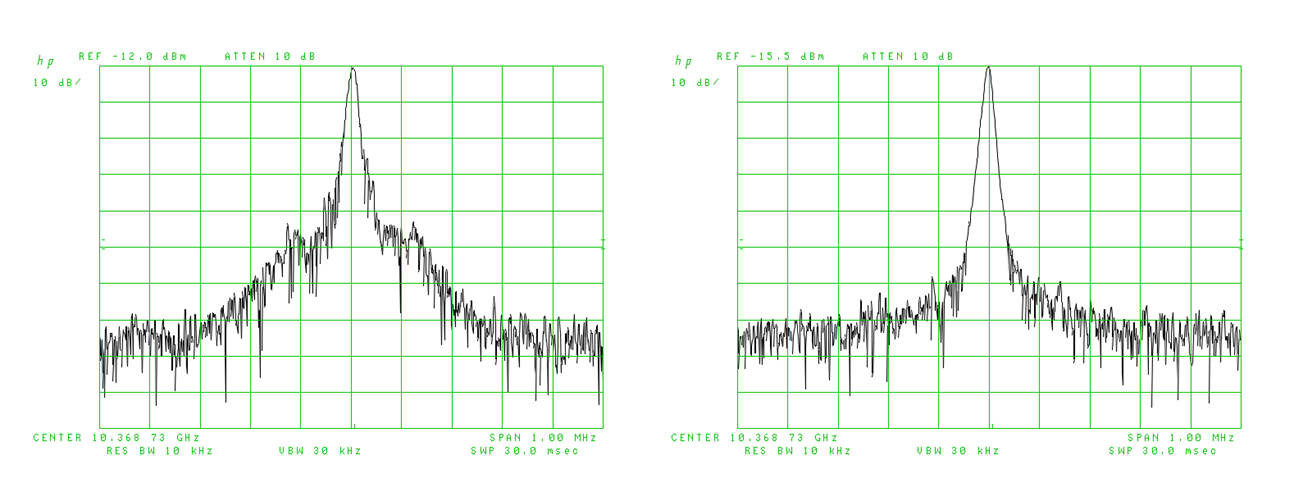
Figure 4: Output spectrum without and with GM8BJF power supply board
The next improvement is to remove the existing reference oscillator and to replace it with the locked Crystek CVHD-950 100 MHz oscillator / ADF4002 combo. Here a board design of PE1PFW was used. As in the case of the microwave synthesizer it is important to use a good low noise voltage regulator. It also turns out that the Crystek VCXO is extremely sensitive to electric and magnetic fields. Without shielding much 50 and 100 Hz interference is present and satisfactory results are not obtained. By building the assembly in a closed tin “Schubert” box all these problems disappear.
To obtain compact results (55 mm * 76 mm) the tin box is divided into two parts. One part for the ADF5355 PCB and the other part for the Crystek oscillator with the ADF4002 PCB as shown in included photos.
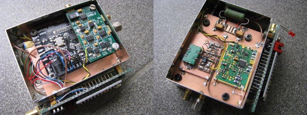
Figure 5: “black” ADF, low noise supply, stabilised Crystek reference and Arduino combined
Further experiments learned that it is not strictly needed to build the ADF5355 PCB in a closed box to prevent 50 or 100 Hz interferences as opposed to the Crystek.
For the loop filter the following components were mounted on the ADF5355 PCB: C11 (27 nF), C12 (400 nF), R11 (200 Ohm), R9 (470 Ohm) and C13 (1nF). There is no need to change these values as with selected chip configuration described above a loop bandwidth of about 20 kHz is obtained. Note that some users have reported other component values of the loop filter, so it is recommended to check the values on the PCB at hand.
An Arduino compatible board is used to set the ADF5355 registers (13 32-bit registers in total). The power supply for this board requires some attention, it is not very critical but sufficient decoupling is needed to prevent noise getting into the synthesizer. The Arduino is also used to read the MUX pin of the ADF5355 to indicate the lock status. So, the Arduino is always on (in fact a regular Arduino program never terminates even when finished execution) which is all the more reason for proper isolation. It is clear that the Arduino should be outside the “RF box”.
When using a supply of 12 V for the system, it is recommended to first step down the voltage to 7 V with an LM317 with quality tantalum decoupling capacitors. Subsequently, this clean 7 V is used to feed both the Arduino and the power supply subsystem PCB with the various low noise ADM7150ARDZ devices.
The presented assembly was measured with results presented in section 4. Phase noise was found to be in line with simulations, as described in the next sections. However, to our surprise, significant PFD (phase frequency detector) spurs were present in the output, way above datasheet specifications, as demonstrated in the figure below. The spurs are only 45 dB down, even with a reduced charge pump current of 0.94 mA.
We received great tech support from Analog Devices to discuss this issue – they ended up loading our configuration (shown on 5 GHz, so without on-chip doubler) on the companies (expensive) evaluation board, showing the spurs about 80 dB down, as expected from the datasheet. Several “black” boards were tried with similar results – good phase noise but unacceptable PFD spurs.

Figure 6: “black” PCB and Analog Devices EVAL board PFD spurs
b. Take 2 – the “greenV2” boards
In our search for results, we opted next to try the “green” boards available on Ebay et al. These recently (mid 2020) appeared in a new version. When testing these boards for the same problem, these were a lot better. Still not the same as the EVAL board, but quite close, and perfectly acceptable – around 65 dB down at +/-2*Fpfd and 70 dB at +/-Fpfd.
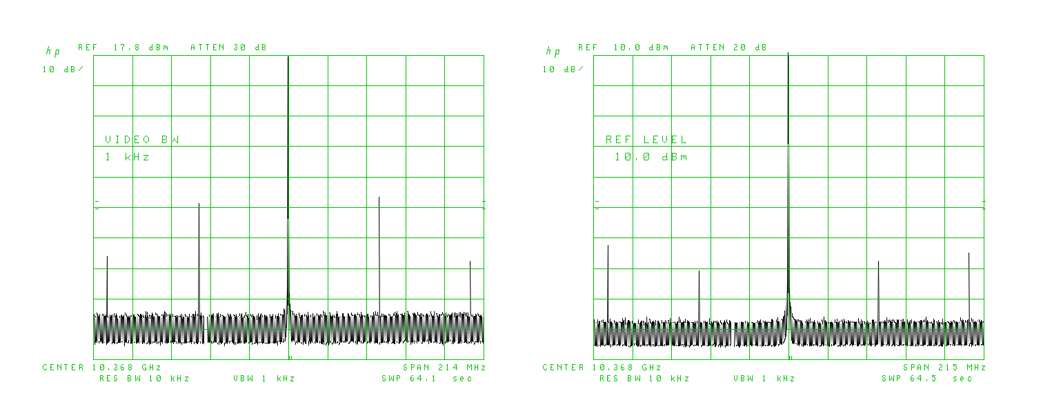
Figure 7: “black” versus “greenV2” PCB PFD spurs (CP 0.94mA)
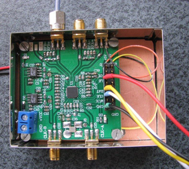
Figure 8: “green” board in tin plate box
4. Measurement results
a. Synthesizer phase noise measurements
The phase detector method described in section 5 was used to assess phase noise. A first test run was to check the simulations done in section 2 but with three different charge pump settings.
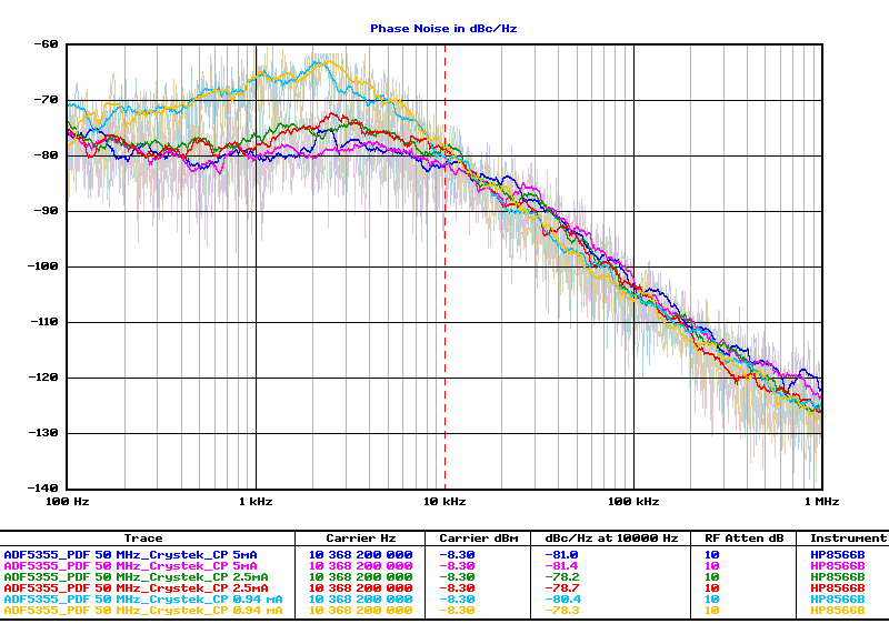
Figure 9: phase noise at various charge pump currents
Analysing the curves of figure 9 for the charge pump setting of 5 mA (or a more correct 4.8 mA) gives the following results. The curve starts at 100 Hz with -75 dBc/Hz. The simulation gave -72 dBc/Hz; so quite similar – our phase noise setup is only good up to a few dB. The plateau between 1 and 10 kHz shows a difference between simulation and measurements of 3 to 4 dB – this is acceptable. A narrower loop filter may be a tad better.
Changing the current of the charge pump to lower values results (as expected) in some more phase noise on the plateau. Also, the shape of the plateau is disturbed as the values of the components in the loop filter were not adapted, with some overshoot present. No attempt is made to correct this as 5 mA was chosen for the charge pump current.

Figure 10: phase noise at various phase detector frequencies
Measurement runs for different PDFs were done and presented in figure 10. The graphs show curves for 10, 50 and 100 MHz PDF. As expected a PDF of 100 MHz is about 3 dB better than a PDF of 50 MHz at plateau level. Since we could not always get a fully stable (digital) lock on 100 MHz PDF we have rejected this approach and 50 MHz is used. The result obtained from using a 10 MHz PDF (without the 100 MHz Crystek) directly from a 10 MHz GPS locked source was also measured and its curve graphed. We expect a curve about 7 dB worse than the 50 MHz curve. There are 2 reasons why the difference is bigger. First of all, the loop filter is not adapted (too much overshoot) and the 10 MHz reference oscillator used was an Isotemp 134-10. The phase noise of this OCXO at 10 kHz is simply not good enough for this application.
These results are sufficient for our further experiments at mm waves the project settled on a PDF of 50 MHz with a loop filter of 20 kHz. If you want to use the board with a 10 MHz PDF directly from a stable source there will be a phase noise degradation, the on-board loop filter needs to be adapted and a very(!) clean 10 MHz source should be used.
b. Multiplier phase noise measurements
For comparison we have carried out some phase noise measurements on our ‘old multiplier boards’.
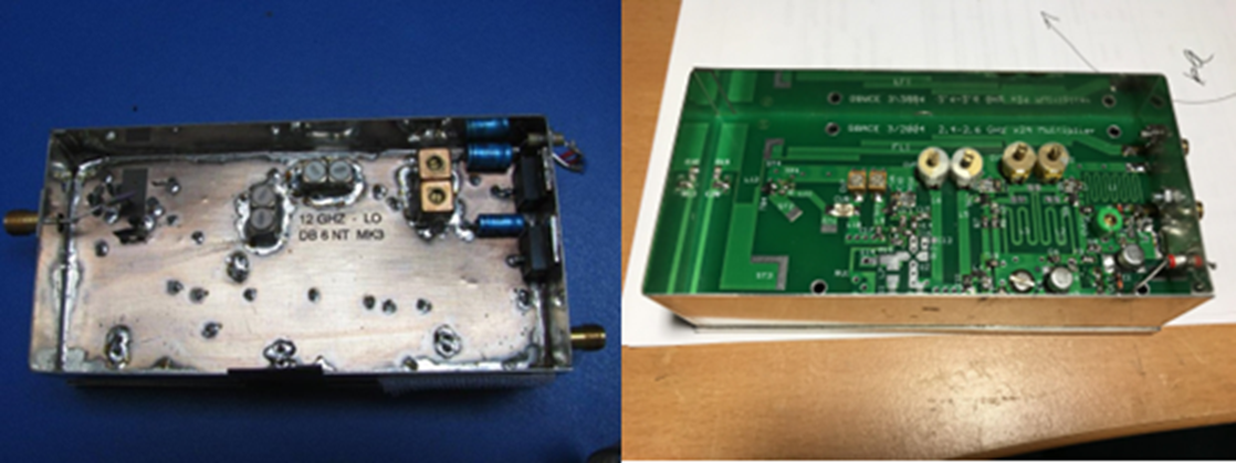
Figure 11: traditional multipliers of DB6NT (*96) and G8ACE (*24)
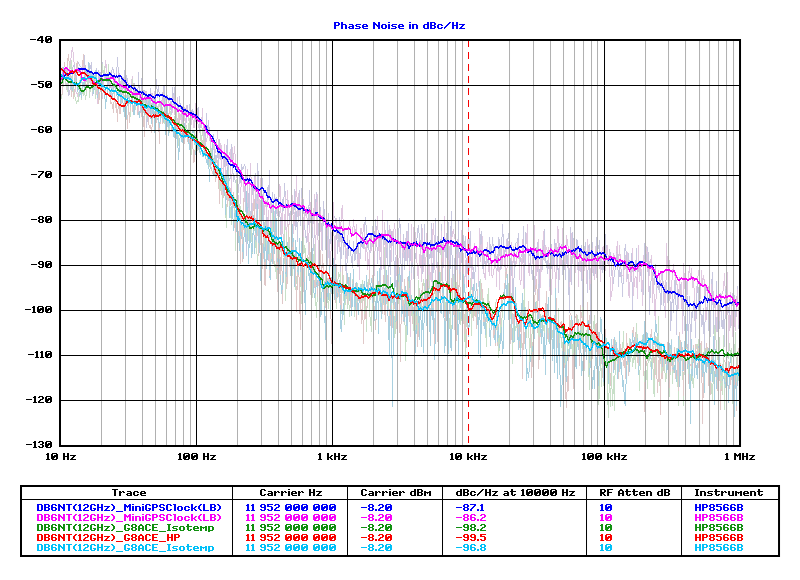
Figure 12: phase noise of traditional multipliers for various clock sources
Figure 12 shows phase noise measurements carried on a 12 GHz multiplier DB6NT MK3 board. The multiplication is 96 from 124.5 MHz to 11952 MHz. As input on 124.5 MHz two different sources were used. First, a G8ACE oscillator locked on a 10 MHz source (Isotemp or HP) and the Mini GPS reference clock of Leo Bodnar. The measured curves show clearly the impact of the quality of the driver for the board. The multiplied XO remains the gold standard (unfortunately also for cost and complexity).
5. Phase noise measurement techniques
Unless you have access to state-of-the-art measurement equipment, measuring phase noise remains a bit of an art. Essentially three methods are available: spectrum analyser measurements, observing the output of a phase detector that locks a reference source and two-channel cross correlation. Two-channel cross correlation uses two phase detector/reference combos and cross-correlates their outputs. Since only the device-under-test noise will be coherent across the two channels, other factors will be cancelled resulting in superior sensitivity at the expense of calculation time (the latter becoming less and less important given advances in CPU speeds). Unfortunately, this type of equipment is not within reach of hams and not yet appearing on the surplus market. That leaves us with the spectrum analyser and phase detector methods, which are rounded out by the excellent software tools of KE5FX.
The spectrum analyser method clearly has its limitations. In the figure below the observation floor of the Hewlett Packard 8568B analyser is indicated by the light blue line. Measuring this is easy: take a clean crystal oscillator, like the calibration oscillator of an instrument (in this case the 100 MHz of an 8566B) that is guaranteed better noise-wise than the spectrum analyser (which is not too hard to find). Then do a phase noise measurement. The result will not be the crystal oscillator but the baseline noise of the analyser that will dominate. So, the direct spectrum measurement of the phase noise of many of our oscillators by a typical ham spectrum analyser is not possible.
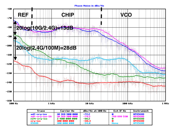
Figure 13: various phase noise plots illustrating baseline and multiplication
a. Phase noise multiplication
However, all is not lost when only a spectrum analyser is at your disposal. Phase noise rises as you multiply the source by a factor of 20log(N), with N the multiplication factor. So, by multiplying our “clean” oscillator to a higher frequency, we can shift the phase noise up into an observable region.
The figure above shows this clearly. The red line is the Crystek at its operating frequency of 100 MHz as measured by the phase detector method, more on that later. Note that even the phase detector method is not able measure the noise directly at 100MHz far away from the carrier due to phase detector method reference (generator) limitations. But, compared to the spectrum analyser noise, the red line is totally below the noise of the analyser. The green line is the Crystek multiplied by 24 (using a G8ACE *24), 28 dB higher at 2400 MHz, it is still mostly below the analyser noise. And our objective system based on the ADF5355 at 10 GHz lifts the noise by another 13 dB. Where the reference noise dominates (close to the carrier), the multiplication factor shows up. In the other zones, where ADF5355 chip and VCO noise dominate, the reference cannot be seen.
b. Offset spectrum measurements
The observant reader will note that a spectrum analyser 8568B is not a microwave analyser and as such the multiplied source cannot be observed directly. Indeed, the multiplied source needs to be “moved” into a region where the SA operates, this case below 1.5 GHz. Fortunately, we know how to do this – a mixer can do this perfectly. But, the LO of this mixer needs to be cleaner than the multiplied source as not to pollute the noise spectrum. This can be a (locked) dielectric resonator or a very stable and multiplied crystal oscillator. In our case we used the 640 MHz output of an 8662A synthesized signal generator that was multiplied by a comb line generator and filtered. This uses step recovery diodes but others like non-linear transmission lines are applicable.
A final note on spectrum analyser measurements is that the all signals involved need to be sufficiently stable at microwaves. If the device under test or the LO drifts, a measurement at an offset of 100 Hz or 1 kHz quickly becomes meaningless – a large underestimation of noise will be the result.
c. Phase detector measurements
The phase detector method is based on nulling the carrier using a double balanced mixer as a phase detector. Both the source under test and a reference signal of identical frequency but 90 degrees out of phase are fed to the DBM. At quadrature, the output of the mixer is a difference frequency of 0 Hz averaging 0 V. The signal that is 90 degrees out of phase is obtained by using the mixer output voltage as input for a phase locked loop that keeps the reference tracking the source under test. Under most circumstances this “error” voltage also represents the combined phase noise of the reference and the source. If the reference is “better” than the source its contribution to the output voltage spectrum can be disregarded. So, we essentially obtain the phase noise spectrum of the source shifted to 0 Hz with everything inside the loop gone, including the carrier. After suitable amplification, using a good LNA, any DC-1 MHz analyser can observe it.

Figure 14: Phase detector method
So, in order to do phase noise measurements at microwaves, we need a down-converter/mixer, a DBM, a PLL to tune our reference, a reference that is as clean as possible and an LNA. Various combinations of carrier noise test sets and tunable low phase noise generators are available to achieve this, accessible at amateur prices at well-known surplus venues.
In figure 13, the phase detector method was used to establish the results for i. the ADF5355 locked to the Crystek CVHD-950, in turn locked to an Isotemp TCXO at 10 MHz (the dark blue line), ii. the Crystek multiplied by 24 locked to an Isotemp TCXO (green) and iii. the Crystek at its fundamental of 100 MHz locked to an Isotemp TCXO (red). The Crystek at 2.4 GHz perfectly matches spec (+28 dB due to multiplication). The Crystek at fundamental matches at 100 Hz and is close at 1 kHz, but further out the fundamental is not able to keep up in our measurement, and the dB difference between fundamental and times 24 becomes smaller. We have arrived at the limits of the generator, which is now noisier than the Crystek, and as such set the limits of our measurement setup. All sources were measured against a HP 8662A/8663A synthesised signal generator, renowned for its phase noise performance. The god-like engineers of Hewlett Packard achieved an incredible typical absolute phase noise spec of -132 dBc/Hz at 1k, -138 dBc/Hz at 10k and around -139 dBc/Hz at 100k for a target frequency 100 MHz … in 1981! These values are indeed close to what we find in figure 13 for direct phase detector measurements of the Crystek performed at 100 MHz (red) as we move away from the carrier.
On a final note – we now have two ways to measure our result at 10 GHz: the offset spectrum measurement and the down-conversion + phase detector method. These are the purple and blue lines in figure 13 and correspond well. Our results are not accurate to a dB but certainly acceptable. The great application notes of HP specify +/-5 dB accuracy as a worst case, and this is confirmed – usually better.
d. Test setup
To produce the phase noise plots as presented in this article, the phase detector measurement technique was used. In the early 80s (1980 that is!), Hewlett Packard released a number of instruments that were groundbreaking and still very relevant today. Our test setup consists of three of these:
- The 8566 (0 to 22GHz) / 8568 (0 to 1.5 GHz) series of spectrum analysers
- The 8662 (0 to 1.28 GHz) / 8663 (0 to 2.56 GHz) low phase noise generators
- The 11729 carrier noise test set. The latter combines a microwave down-converter, a mixer, and phase locked loop and a low noise amplifier.
When complemented by the excellent software program of KE5FX John Miles for spectrum analyser control, a nice self-contained phase noise measurement system can be built based on these three pieces of equipment, as depicted in figure 15. It is bulky and noisy, but very accurate and best of all, still serviceable as opposed to today’s equipment. The generator provides not only the reference to the DBM, it also delivers an ultra-clean 640 MHz signal that is multiplied in the carrier noise test set using a step recovery diode (SRD) and filtered and thus provides the LO for microwave downmixing in the test set. The loop is then closed by pulling the base crystal oscillator of the generator. We have built 2 test setups, as to eliminate equipment errors, providing identical results. Our measurements are presumed good to +/- 3 to 4 dB.

Figure 15: Measurement setup as used
6. On the air
The following setup was used to view and listen to the signal at 10 GHz.
Transmitter: ADF 5355 as described on 10368.2 MHz.
Receiver chain: a DB6NT 10 GHz MK3 (XO 106.5 MHz stabilized with ADF4002 PLL) with IF output at 144 MHz. Microwave Modules converter to 28/30 MHz and RFSpace SDR-IQ for analysing the signal and a Kenwood TM-255A/E for listening.
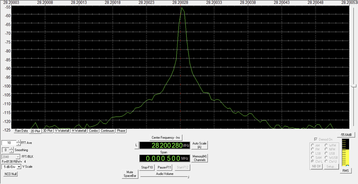
Figure 16: 500 Hz of carrier spectrum of the ADF5355 as observed on SDR-IQ
Listening to a carrier on the TM255 gives a clear T9 tone. At zero beat some ‘flutter’ was observed. This ‘flutter’ is the result of the different oscillators and PLLs in the receiver and transmitter chain. Being at a very low level it will not have influence on the quality of a CW, SSB or digital transmission.
Microphony is another aspect. Tapping with a screwdriver on the Crystek VCO compartments and on the ADF PCB was of course noticed at the receiver side, but for normal operation this should not be a problem. On the other hand, if used in an enclosure in a mast it is advisable to take precautions to avoid wind modulation. At 24 GHz the microphony effect is stronger and also the SMA connectors must be tightened to avoid annoying creaking. Also, the microphony effect at 24 GHz of the coaxial cables should not be forgotten.
The measured output at ‘RF output B’ is a few dBs lower than the figures in the datasheet, which are measured at the official Analog Devices ADF5355 evaluation board. Probably some tuning is needed, but this was not further explored. Also, the used PCB material is not RF quality.
7. Discussion and conclusion
The advent of microwave synthesisers in the tens of GHz range, such as the ADF5355 and the LMX2820 is changing the way microwaves are generated. It eliminates the complex and bulky multiplier chain as well as the crystal oscillator. From a practical perspective, good care and feeding of the synths is critical, and not all cheaply available boards are created equal. With correct system design and good execution (reference!), solid end results can be achieved. The ADF5355 or its successor 5356 will be a cornerstone of our next gen 10-100 GHz experiments.
8. References
Some interesting phase noise numbers for our microwave LOs
- G8ACE DF9LN See http://millimeterwave.free.fr/Phase_Noise_F.htm
- 9912 DDS http://www.qslnet.de/member1/on4iy/9912.html
- DigiLO http://q5signal.com/image/catalog/digiLO%20Doc%2017_8_3.pdf
Phase noise reading – highly recommended
- 8862/3A http://www.ke5fx.com/stellex/5952-8217.pdf
- PD method http://www.thegleam.com/ke5fx/gpib/5952-8286E.pdf
- FD method https://www.hpmemoryproject.org/an/pdf/pn11729C-2.pdf
Crystek LO lock
- PE1PFW design http://pe9ghz.org/cmsms/index.php?page=lo-locking